
Close-up of sign with logo at Silicon Valley headquarters of technology company Synopsys, Mountain View, California, May 3, 2019. (Photo by Smith Collection/Gado/Getty Images)
Synopsys created a buzz in 2020, and now Google, NVIDIA, and Cadence Design have joined the party. What lies ahead?
Introduction
Designing modern semiconductors can take years and scores of engineers armed with state-of-the-art EDA design tools. But the semiconductor landscape and the world around us is being revolutionized by hundreds of new chips, primarily driven by AI. Some entrepreneurial thought leaders believe that the expensive and lengthy chip design process could shrink from 2-3 years to 2-3 months if hardware development was to become more agile, more autonomous. And chief among a new breed of agile design tools is AI itself.
The Semiconductor Design Landscape
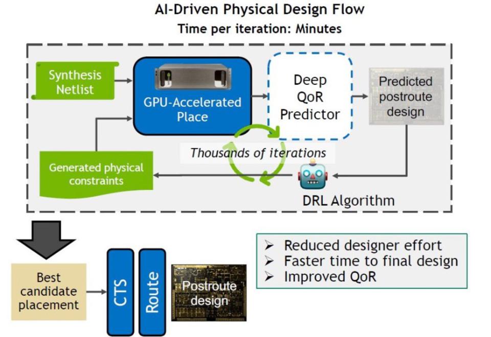
This discussion began in earnest when the EDA leader Synopsys announced DSO.ai, Design Space Optimization AI, an software product that could more autonomously identify optimal ways to arrange silicon components (layouts) on a chip to reduce the area and reduce power consumption, even while increasing performance. Using reinforcement learning, DSO.ai could evaluate billions of alternatives against design goals, and produce a design that was significantly better than that produced by talented engineers. The size of the problem/solution space DSO.ai addresses is staggering: there are something like 1090,000 possible ways to place components on a chip. That compares to 10360 possible moves in the game of Go which was mastered by Google AI in 2016. Since reinforcement learning can play Go better than the world champion, one could conceivably design a better chip if one is willing to spend the compute time to do it.
Results are quite impressive, realizing 18% faster operating frequency at 21% lower power, while reducing engineering time from six months to as little as one. In a recent interview, Synopsys’ Founder and Co-CEO Aart de Geus disclosed that Samsung have a working chip in-house today that was designed with DSO.ai. This would indeed be the world’s first use of AI to create a chip layout in production – from RTL to tapeout.
Recently Google published results of doing something similar, as has NVIDIA. And Cadence Design Systems just announced an AI-based optimization platform similar to Synopsys DSO.ai. Before we take a look at these efforts, lets back up a little and look at the entire semiconductor design space. A good place to start is the Gajski-Kuhn Chart that outlines all the steps of chip design along three axes: the Behavioral level where architects defines what the chip is supposed to do, the Structural level where they determine how the chip is organized, and the Geometry level where engineers define how the chip is laid out.

All semiconductor design teams work along three axes of specification: what do you want the chip to do, how will it do it, and how will you build it. Each step feeds the next step in a spiral. source: Synopsys
Based on this model, each step towards the center (which is when the team “tapes out” the chip to the fabrication partner) feeds the work in the next phase in a clockwise direction. To date, all the application of AI has been in the geometry space, or physical design, to address the waning of Moore’s Law.
Synopsys DSO.ai
As I covered at launch, Synopsys DSO.ai was the first entrant to apply AI to the physical design process, producing floor plans that consumed lower power, ran at higher frequencies, and occupied less space than the best an experienced design could produce. What really attracted my attention was the profound effect of AI on productivity; DSO.ai users were able to achieve in a few days what it used to take teams of experts, many weeks.
Google Research and NVIDIA Research
Both companies have produced research papers that describe the use of reinforcement learning to assist in the physical design of the floor plan. In Google’s case, AI is being used to lay out the floor plan of the next generation TPU Chip and the company is investigating additional uses of AI such as in architectural optimization.
NVIDIA similarly has focused on that same low-hanging fruit: floorplanning, and with all the compute capacity they have in-house, I’d expect NVDIA to continue to eat their own dogfood and use AI to design better AI chips.
Similarly, NVIDIA has used the company’s GPUs to optimize floor planning for a future GPU chip. source: NVIDIA
Cadence Design Systems Enters the Market
Cadence has recently launched their “intelligent chip explorer” called Cerebrus to optimize the physical design process with reinforcement learning. Not to be confused with the Wafer Scale Engine AI maker “Cerebras”, the newly announced platform looks similar in capability to the DSO.ai that Synopsys launched in March 2020, focusing on physical design. While Google and NVIDIA may have sufficient resources and skills to develop their own AI for design optimization, the majority of semiconductor companies and projects will select a tool from an EDA vendor. Cadence’s entrance seems to solidify the reinforcement learning technique as the next big shift in design methodology. We believe AI will become pervasive as designers become more comfortable with letting the machine determine the layout, and competitive pressures mount.
Conclusions and Outlook
The excellent research being conducted at NVIDIA and Google will reinforce the message to designers that they should rapidly consider AI-led optimization to improve performance, cost, and energy consumption. NVIDIA and Google are undoubtably focusing this effort to produce better GPU’s and Cloud TPU platforms to enhance their competitive position. We think rumors to the effect that these companies might enter the EDA tools market are off base: the AI optimization is a tool they use to help improve their own products and services.
Cadence Design System’s entry has validated the approach as well, and the industry momentum will now accelerate. However, Cadence is just beginning the journey, while Synopsys enjoys the pole position, with at least a full year head start: Synopsys customers such as Samsung already taping out designs that were created with DSO.ai.
Now the question becomes, what about “The Rest of the Story”? Using AI in physical design is great, but in our view, it is only the beginning, representing perhaps only 10% of the opportunity. There are rich fields to harvest along the Behavior and Structure axes, which will create a spiral of optimization across the design workflow. We look forward to hearing what Synopsys co-CEO Aart de Geus has to say on this topic when he presents the Keynote speech at the upcoming HotChips conference on August 23.
Stay tuned!