IBM Research has been working on new non-volatile magnetic memory for over two decades.
Non-volatile memory is wonderful for retaining data without power, but it is extremely slow, and does not last forever. Primary computer memory (Dynamic Random Access Memory, or DRAM) is fast but volatile (thats the D part), and on-processor chip memory (Static Random Access Memory, or SRAM) is extremely fast, but is not as dense as we would like. Technology, like life itself, is full of compromises. But, …
Wouldn’t it be nice if computer memory was non-volatile, dense, fast and durable? High-Performance Computing (HPC) and Artificial Intelligence (AI) applications would run faster, and consume less power. And main memory itself could be non-volatile. Well, that day may be closer than you might think.
A team of IBM Research scientists has been working on Magnetic Random-Access Memory (MRAM) for decades. Early MRAM had significant performance and manufacturing limitations, but now these scientists believe they are close to inventing something closer to memory nirvana. Ok, perhaps something short of Nirvana, but closer. If these scientists are correct, they could revolutionize storage for on-processor last-level cache memory and faster non-volatile memory (NVM) on edge devices. Let’s look at why IBM is so excited about this advancement and what it will take to finish the job. We have also published an in-depth report here.

IBM foresees a memory technology that could be fast, dense, non-volatile and durable. (Photo by
The Promise of STT-MRAM
IBM is developing a technology called Spin-Transfer-Torque MRAM. On-processor SRAM memory offers exceptional bandwidth at low latencies, providing a fast cache between DRAM and the processor cores. However, while SRAM is fast, it is not particularly dense, limiting the size of SRAM caches to hundreds of megabytes. Meanwhile, emerging applications such as AI accelerators demand more memory capacity and MRAM could double that capacity at low power and unlimited endurance if a much faster version were available. In this world, ASICs such as AI accelerators could increase performance with more on-chip memory for model weights and parameters. Accelerators needing more memory capacity could also benefit from the reduced frequency of DRAM accesses a larger cache could provide.
MRAM Applications
BM envisions four eventual markets for STT-MRAM. The first is what most of us think of as stand-alone memory. STT-MRAM could one day even replace DRAM in applications requiring non-volatility. The second market is for embedded non-volatile memory in chips, where Samsung is already fabricating STT-MRAM on 28-nm Silicon on Insulator (SOI) manufacturing lines. Cache memory on slower low-power processors such as used in mobile phones is the third market opportunity. The fourth and largest market opportunity is to replace some SRAM for high-performance computing and Artificial Intelligence as a last-level cache.
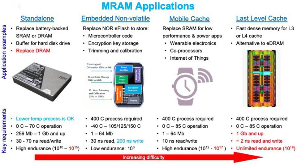
IBM envisions four markets for STT-MRAM once the research is complete. Source:IBM
Everspin Technologies has effectively shipped all early STT-MRAM devices into the market thus far, targeting high-end ultra-reliable storage buffers. IBM’s FlashCore module uses this technology today. However, to target the larger market of last-level cache, IBM will need to improve the read-write time from 30-70ns to something like 2ns. And STT-MRAM endurance would need to improve from the current 1010 writes to virtually unlimited data retention, or something like 1018 writes (is that an “Exa-Write”?).
The Challenges of STT-MRAM
Five challenges below could enable last-level cache memory and embedded flash. IBM Research had previously solved the first four challenges, the most advances occurred in 2020. Only one issue remains unsolved to date: IBM must figure out how to reduce the current needed to switch states by about 50%.
- The time it takes to switch states must be fast, in the 2-3 nanosecond range.
- The switching must be reliable, down to 1e-9 write error rate.
- The switching voltage distribution must be in a tight range for consistent operation.
- The fabrication process must be possible on the advanced process nodes used in microprocessors, currently in 5 or 7nm.
- The current required to switch states must be low, about ½ what is presently possible.
Conclusions
Memory technology changes have slowed dramatically over the decades. Core memory was invented in 1964. Then DRAM was invented by Bob Dennard of IBM in 1966. SRAM was invented in 1969, and the first Intel DRAM chip shipped in 1970. NAND flash memory was developed in 1980. However, since these remarkable inventions, changes over the last four decades have been primarily enabled through VLSI manufacturing advancements, not fundamental shifts in the physics of a memory cell.
With STT-MRAM, we are finally looking at an entirely new implementation of a one and a zero. Faster, cheaper, denser, and durable non-volatility combined in a single memory design. STT-MRAM will not replace everything, at least not anytime soon. Level 1 and level 2 cache will remain implemented in SRAM, at least for now. And NAND flash memory will remain the king of the NVM hill for low-cost and high-density. But STT-MRAM may soon challenge existing memory devices in Level 3-4 caches and embedded flash. DRAM could also be built with STT-MRAM where non-volatility is required.
It has been a long journey for many at IBM Research, but success is finally in sight.